Home · Book Reports · 2017 · FPGA 101 - Everything You Need to Know to Get Started
- Author :: Gina R. Smith
- Publication Year :: 2010
- Read Date :: 2017-12-02
- Source :: (2010) FPGA_101_Everything_you_need_to_know_to_get_started.pdf
designates my notes. / designates important.
Thoughts
It got me up to speed with most FPGA terminology. I was tinkering with Quartus 2 (10.1sp1) as I read the book. It is different than the Xilinx ISE examples, but similar enough to make sense of. After writing and simulating a few very simple designs I now have the confidence to tackle a more detailed look at the VHDL language as well as the more advanced features of Quartus.
Even though this was my first foray into FPGA/VHDL, it seemed to be very easy to understand (with a background in electronics and programming).
At the same time I was reading this I watched the first 11 videos in a similarly styled VHDL tutorial from Eduvance. This series also focuses on Xilinx, but the majority is presented in a manufacture agnostic manner. I will definitely be watching the remaining 14 videos as I work my way through another, more intermediate, VHDL book, (2011) VHDL 101 Everything you need to know to get started. (an excellent follow up)
Bruce Land at Cornell has videos from his FPGA/Verilog course, ECE5760 DE2/115 lectures 2011, available on youtube. This is quite a bit more advanced, but I found the first 6 lectures easy to follow alongside reading this book, even though it is Verilog and not VHDL.
Table of Contents
-
01 - Getting Started
02 - Simple Designs
03 - FPGA Development Phases
04 - Design
05 - Simulation
06 - Synthesis
07 - Implementation
08 - Programming
Appendix 1 - Test Benches
· CHAPTER 1: Getting Started
page 12:
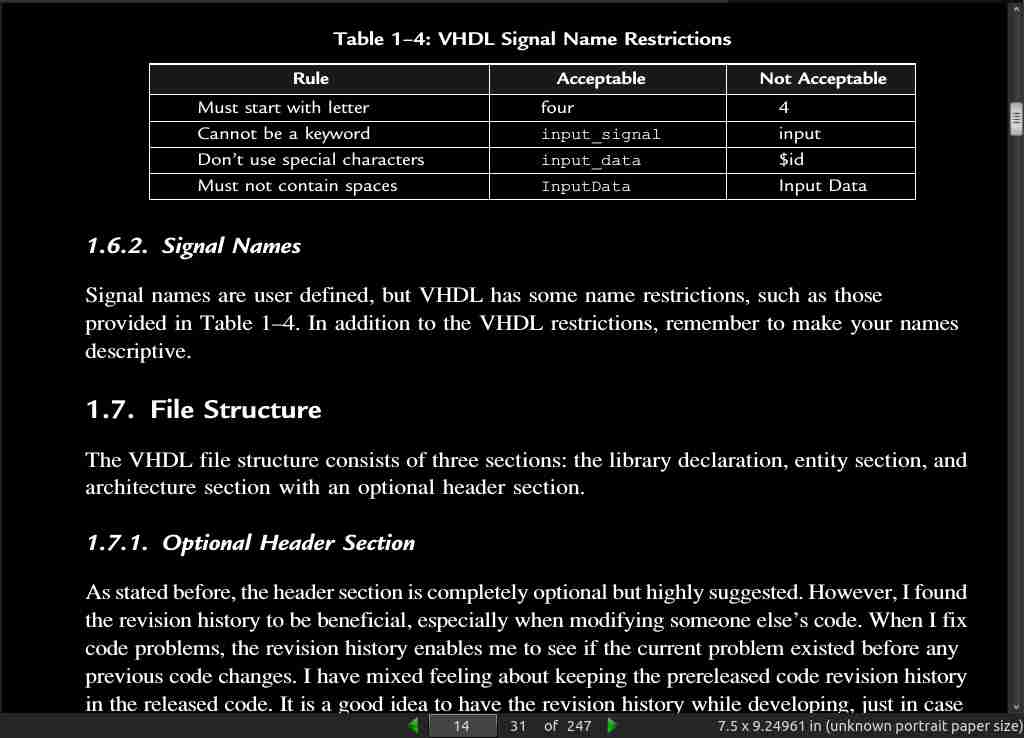
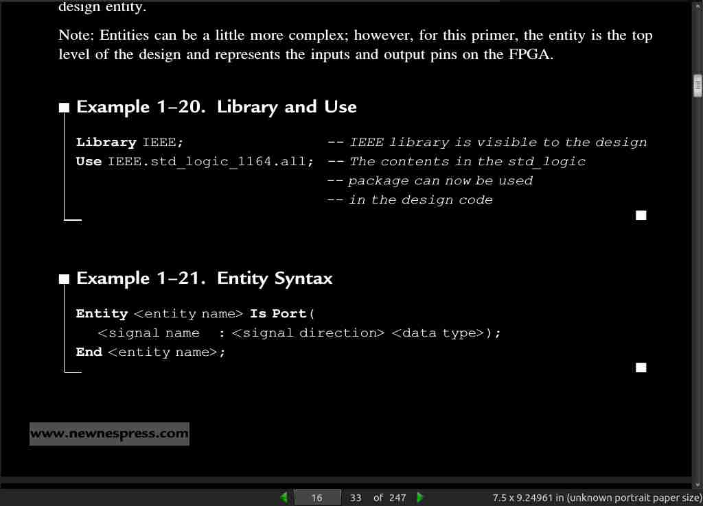
- signals represent some kind of data. They are assigned a name and data type. The basic signal syntax follows:
Signal <signal name>: <data type>;
-
You can use signals in mathematical equations, to assign values, to connect other signals, and to store values in them.
-
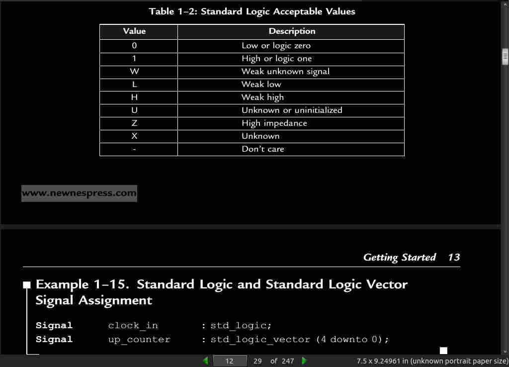
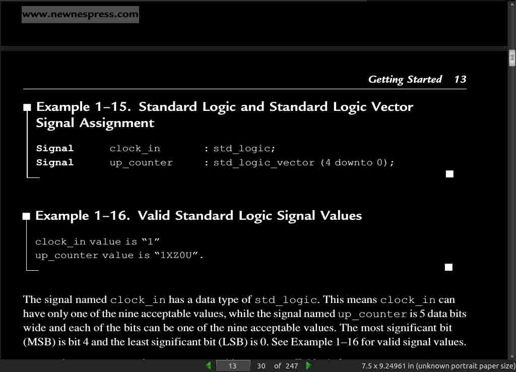
The VHDL data are of a specific type such as std_logic, std_logic_vector, bit, bit_vector, or user defined. Std_logic is read as standard logic and std_logic_vector as standard logic vector. Bit and bit_vector are read as written.
-
Std_logic signals represent one data bit and std_logic_vector represents several data bits.
page 13:
- Bit and bit_vector have two acceptable types, see Table 1–3.
page 14:
page 16:
page 18:
-
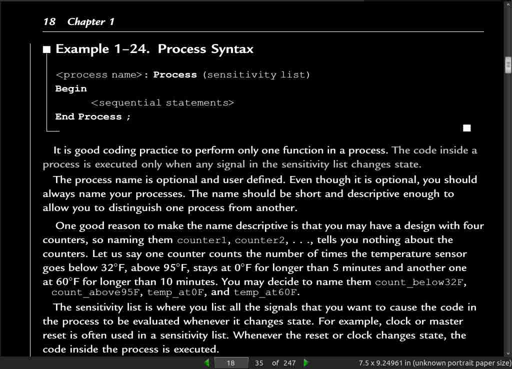
The code inside a process is executed only when any signal in the sensitivity list changes state.
-
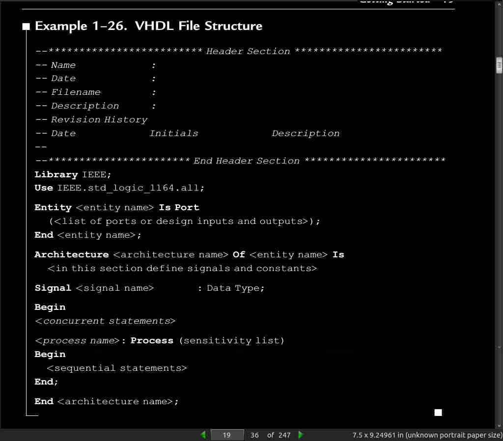
Concurrent statements are outside of processes and executed or updated at any time any of the signals changes, see Example 1–25.
page 19:
page 29:
· CHAPTER 2: Simple Designs
page 30:
- In VHDL, entity signals defined as outputs can only be assigned values and cannot be used for things like conditions or calculations.
page 32:
- The shift register signal assignment can be written using one signal statement; however, the operator for that assignment is not discussed in this book.
page 36:

page 37:
- The read command is defined in the std.textio package in the std library.
· CHAPTER 3: FPGA Development Phases
page 44:

page 54:
- The three basic FPGA architecture elements are I/O interfaces, basic building blocks, and interconnections.
page 55:
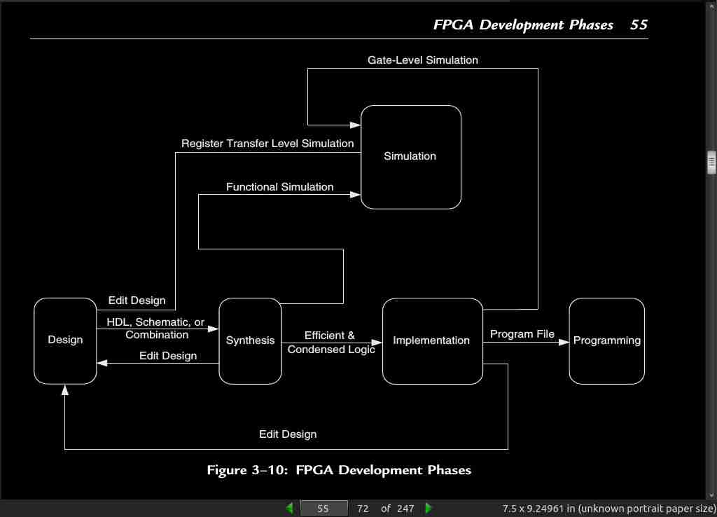
· CHAPTER 4: Design
page 60:
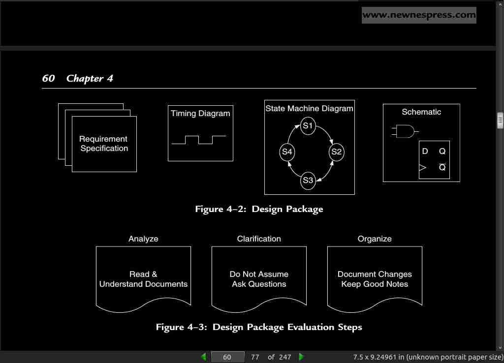
page 72:
- Example code for a pulse detector/verifier.
· CHAPTER 5: Simulation
page 117:
- Xilinx ISE simulation tutorial using ModelSim XE III 6.4b.
· CHAPTER 6: Synthesis
page 151:
-
…standard for derating the internal resources. Most of the time 60–70% is a good range. I generally like 50%, especially for new designs, where there is a good possibility that the design will grow.
-
Additionally, it is always a good idea to derate input/output pins to accommodate potential growth.
· CHAPTER 7: Implementation
page 161:
-
Implementation, also referred to as place and route (PAR)
-
Implementation is the process that maps the synthesized netlist to the specific or target FPGA’s resources and interconnects them to the FPGA’s internal logic and I/O resources.
· CHAPTER 8: Programming
page 197:
-
Tip 1. When daisy-chaining devices, make sure to add the ability to jump out or remove any of the devices, if necessary. Sometimes, a device may cause problems, and having the ability to remove it from the chain helps in isolating the problem.
-
Tip 2. It is always a good idea to design in some debugging and troubleshooting mechanisms, such as test points, pads, or connectors. Most likely, a logic analyzer will become your best friend for verifying, troubleshooting, or just working with the design. Consider using test connectors that mate with lab equipment hardware. This makes your life so much easier. One of my favorites is a Mictor connector that mates directly with Tektronix’s logic analyzer. This made life so much easier than having flying leads soldered to the board. Plus, with surface mount packages, probing is very difficult and, in some cases, impossible. The test connector can always be removed from production boards. As shown in the simulation phase, lab data can be read into a testbench using a connector, like a Mictor, which makes capturing the data a lot easier.
-
Tip 3. Many FPGAs require several different voltages (such as supply or signal), so be sure to consult the datasheet for the acceptable ranges and the appropriate supply capacitors.
-
Tip 4. Sometimes, it is desirable to select a specific FPGA package based on the ability to upgrade to a larger size (more internal resources) in the same package without respinning or re-laying out the board. If this is the case, then make sure the two devices are pin-for-pin compatible. The power and grounds may be in different locations. So, if the plan is to start with one specific FPGA size with the goal of being able to replace it with a larger size without having to redo the board, at a minimum, make sure both selections are pin compatible and have the same voltage requirements.
-
Tip 5. If you have unused input pins, make sure to read the user’s guide, application notes, or other appropriate material to determine if it is necessary to connect them to a known state. This can be as simple as making a selection in the implementation tool. Although this is simple, it does require some action on your part.
Appendix - 1
- test benches